Some types of distortion found in sound systems, other than misuse, feedback, reflections or the resonance of speaker cabinets, windows, floors, tone arms, etc, can comprise;
Instabilities | 'Paranormal' Audio | A Tip
Using good quality audio equipment of, say, early '80s vintage a record deck could produce 3-6% with 8-10% being typical, even with the best cartridges and records. A reel-to-reel tape deck would give 2-3%, cassette decks doubling this although the variation between individual cassettes was much greater. Tuners gave some 0.2-1% providing the highest quality source for domestic users. Monitor quality speakers giving say 80dB @ 1W would produce about 0.3% in the mid-range and 1-2% at lower frequencies.
When fed with a signal, some parts of an amplifier's circuitry will resonate at multiples, or harmonics, of the input signal. THD, or total harmonic distortion, is often cited in the specification of an amplifier and is seen by many as a measure of how well an amplifier performs. Two graphs, below, show how a single figure (in this case <0.1%) stated in a specification can be meaningless when the THD can vary considerably with load and frequency.
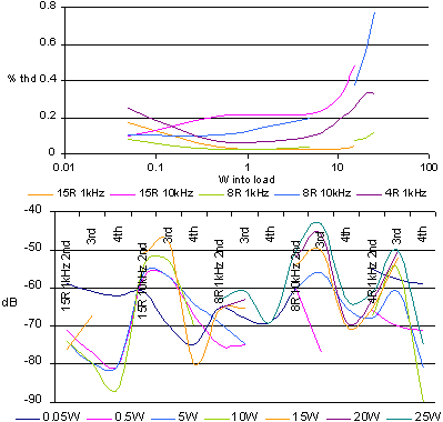
0.1% seems not only arbitrary but optimistic as well. Note how 3rd, and therefore odd, harmonics predominate at higher frequencies. These are more noticeable and considered more objectionable than 2nd harmonics which are interpreted as having a 'musical' and therefore acceptable quality. A very rough rule of thumb multiplies the THD by three at 20kHz, when quoted at 1kHz.
Temporal aspects of audio processing, inherent in hearing, produce pronounced variables in perception. For example, long periods of high distortion are more objectionable than short bursts and longer term exposure to a specific level increases sensitivity. At the same time, THD peaks at low frequencies are far more difficult to detect than those of the same amplitude in the mid-range.
Most THD measurements are made using a continuous sine wave and take no account of performance when the amplifier is driven by other waveforms or transients normally found in music. The human ear is less sensitive to harmonic distortion than it is to other forms and this is why some specs will provide maximum output ratings at 10% THD.
When driven by a signal with sharp rise and fall times like a square wave 'overshoot' can be observed.
Caused by a transistor's parameters inconvenient habit of changing with collector current, most would agree that this problem can be rendered inaudible if the amplifier is designed to be sufficiently fast, or operated in class A, eg;
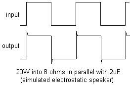
Simulated loads may have very little in common with reality given the very lively reactance represented by some speaker enclosure designs, their associated cross-overs and 'low-loss' wiring. Jim Lesurf, a designer with Armstrong, has an excellent site where he mentions 'The Society for Cruelty to Amplifiers'.
Intermodulation problems can arise when a power amplifier's output 'lags' behind a fast transient that appears at it's input, the resulting feedback creating a distortion that the ear is as sensitive too as cross-over distortion. This problem can be overcome by making each successive stage of an amplifier faster than the preceding one and by using a low-pass filter at the input. It is for this reason that the class A pre-driver usually found in a power amp design has to be the fastest, or selected for a very low base capacitance. High voltage types are recommended.
A 'good' slew-rate for 20kHz at 100W into 8 ohms is usually considered to be 20V/µS or better. Some designs exceed this by a considerable margin. Smaller amplifiers do not have to slew so quickly, so a similar 50W amplifier needs 14V/µS and a 20W amp 9V/µS. If an output stage uses 'slow' transistors (say 800kHz) a marked improvement in high frequency performance will be produced by replacing them with 'fast' ones (say 4MHz+), often accompanied with a distinct drop in the THD.
Experience has suggested that, when comparing two amplifiers, one with 0.03% THD and 0.01% IMD will sound better than another with 0.01% THD and 0.03% IMD.
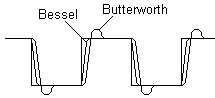
Normally, a low roll-off Bessel filter is placed at the input so that the phase shift is proportional to frequency, causing the time lag to be the same for all frequencies, with no audible consequences ('ringing').
Such a filter can be useful in blocking RF breakthrough.
With some capacitive loads, ringing caused by the inductor in series with the output (intended to counteract this problem) can be reduced if the coil is replaced with a low-value, say 0R22, non-inductive, heavy-duty resistor. 'Super' speaker cables can be major contributors to this kind of problem and are best avoided.
With large output voltage swings, time delays taken by the capacitor decoupling the AC feedback loop to charge and discharge can modulate the output.
A detailed manufacturer's discussion of steps taken to reduce TID can be found here.
This occurs when the amplifier is driven so hard that, in effect, it runs out of power supply, the peaks of the signal then being cut off, or clipped. Overdriven (usually) speaker cones, still moving, 'overshoot' thus producing objectionable harmonics. It is this particular distortion that has most people rushing to 'turn it down' and quite rightly too since silence will usually follow.
The same result occurs when some protection circuits kick in, especially those triggered by an over-current condition through the output device's emitter resistors when using reactive loads that dip below a couple of ohms or those that generate a back EMF. It is for this reason that an upgrade to a new speaker especially a low impedance one, and/or 'strange' cables, may prove unsuccessful and, in the worst case, disastrous. It is wise to try a given amplifier / speaker combination at the highest volumes that can be more than reasonably expected before commiting to an expensive purchase. If in doubt, fit a low resistance, say 1R, or suitably rated bulb in series with the load.
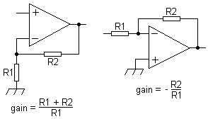
Each time an amplifier output of non-inverting or inverting configuration crosses zero a point is reached when 0V occurs across the feedback resistor (R2 below). Since no current flows the amplifier then 'sees' an infinite resistance, altering the gain characteristics of the circuit. In reality, this phenomenon is usually ignored by designers.
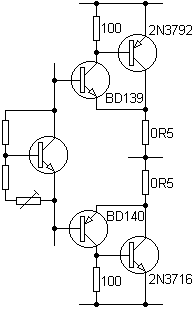
The circuit found strung between the bases of the driver transistors 'ties' them together so that the output does not pass destructive amounts of current. It does, however, allow a little current (quiescent) to flow so that the output devices are biased on. A well-used example is shown below:
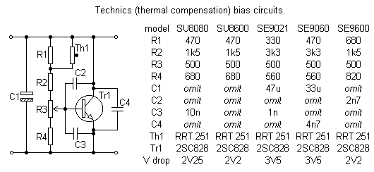
Sometimes described as a 'variable zener' or 'amplified diode', it can also be used to reduce the overcurrent conditions that arise with hot bipolar output devices (NTC, negative temperature coefficient). If the transistor is put in close proximity to a heat-sink, output device or, sometimes more conveniently, bonded to a driver, closer thermal tracking can be obtained. Some prefer to fit a resistor between the transistor's base and collector to overcome potentially destructive wiper open-circuits.
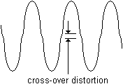
The time it takes for the output of the amplifier to swing or slew across this small voltage drop, as it approaches zero, gives rise to cross-over distortion which can be seen easily on an oscilloscope.
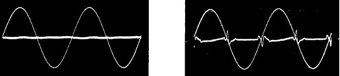
Subtracting the input from the output and imposing this on either can demonstrate and pinpoint not only inadequacies but improvements too (Technics 'New Class A' on left, class B on right).
Alternatively, using the input of the amplifier as the x axis, and the output as the y and adjusting the respective amplitudes, a perfectly behaved amplifier will give a straight line at 45°, cross-over distortion appears as a kink in the middle (positive-going for class AB, negative for class B). Adjust the bias setting (R3) for minimum distortion at progressively higher output levels and higher frequencies. Clipping, if desired, and the effects of filters and tone controls can also be displayed, some very interesting results being obtained from some very well-known makes!
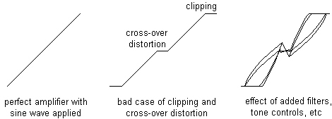
It was cross-over distortion that distinguished, in sonic terms, early solid-state designs from their thermionic equivalents. This was described as "the transistor sound" — a quality of sharpness and crispness that, allegedly, makes valves sound muddy by comparison. Interestingly, it has been noted by the author, and others, that cross-over and other types of distortion become audible at the same time they become visible on a 'scope.
It has been noticed that many manufacturers insist on using a low quality open carbon skeleton preset pot to adjust the quiescent current. These are prone to corrosion and open circuits that can then destroy an output stage. It should be noted also that a carbon pot can exhibit 10 times the thermal drift of a comparable cermet type. Given the cost of the output devices alone care should be exercised to avoid unnecessary failures and quality sealed types should be specified and used to replace older ones. If the wiper has multiple contacts this will enhance performance.
The layout of an output stage can affect the stability of the bias and J. N. Ellis drew attention to this (EW&WW,1/91). The quiescent flow in the 0R5 resistors (below) will rise as the Vbe of both output devices rises. This can cause an increase in a driver's Vbe giving a 4mA increase per °C rise per pair. With two pairs this is doubled, as does each driver's Vin.
Typically, in a conventional Darlington circuit, the output base resistors are 100R, the quiescent current 50mA and driver current about 6mA. At room temperature the Vbe of the output devices will be about 0V55 and that of the drivers 0V65.
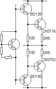
The bias transistor may be passing 10-15mA and then will have a higher Vbe than the drivers. A voltage drop of, say, 2V4 will be required and the bias transistor will be operating with a Vbe some 20mV higher than the driver. 2V4 / 0V67 is only 3.58 when a value of 4 is needed to be thermally stable.
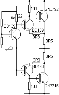
With a higher-power bias transistor, with a larger emitter area, the Vbe at the same emitter current will be lower. Inserting a resistor in the collector increases the bias voltage needed whilst any drift will be transferred to the output devices. Suppose the bias current is 12mA and 4Vbe = 2V68 bias. Rc then = (2V68 - 2V4) / 12mA = 22R, a larger value then over-compensating. In a complementary Darlington stage, small resistors in series with the driver's emitters will raise the bias voltage needed. At 6mA 3R3 will suffice, the loss at peak drive, say 200mA, giving an acceptable 0V66. Higher values will increase the compensation. Thermally coupling the bias and driver transistors will then prevent thermal runaway, eg;

As the output device Vbe falls with increasing temperature, the driver current decreases slightly while the output current increases slightly and must be taken into account when designing the bias circuit for the maximum temperature range anticipated for the amplifier. The above can be used to modify an existing design. Compare to PMI, Giesberts IGBT and Stochino. For new builds M. Renardson offers another approach with 'A New Audio Amplifier Circuit Design'. A quasi-complementary output stage can ease output device selection and reduce costs, it being easier and cheaper to produce PNP devices in germanium, and later, NPN in silicon which could run hotter. A drawback encountered with this arrangement is that the transfer characteristic can become markedly assymetrical at low signal levels, then contributing to distortion. For this reason, low-level distortion figures are usually absent from an amplifier's specification.
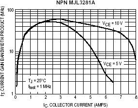
The use of feedback, say, the use of a RC network between the input of the class A driver stage and the output (see TID discussion above) with conventional external feedback will reduce cross-over distortion considerably, or it can be eliminated if the output stage is fast enough to render this transition inaudible or if the quiescent current drawn is high enough for the output transistors to continuously operate in their linear fT regions (class A - see MJL3281A graph above). The low-level distortion found with other types of amp will also be eliminated. Power supplies and heat-sinking will, however, then have to be commensurately larger to sustain these very large losses, efficiency becoming a minor consideration.
'New Class A' was intended by Technics to impart the low-level distortion of class A with the efficiency of class B. This was achieved by clamping the driver bases so that the output devices conducted over the transition period. The result impressed this author, and many others.
With a class AB configuration, the driver stage will often drive the load in class A mode up to a low output level, say 2½W, beyond which the main output devices will kick-in providing higher drive. On the central part of the transfer characteristic where both output transistors are conducting the mutual conductance (gm) doubles. When one of the output devices cuts off as the circuit goes into class B mode the abrupt change in the slope of the transfer characteristic can produce a considerable rise in distortion.
Class B amplifiers, probably the commonest format seen, rely on a small quiescent current through the output devices to overcome transition phenomena although some designs will have none. Usually reserved for low-quality builds, some very famous and desirable amplifiers have operated in this mode.
In class C designs, where the cross-over transition can be comparatively quite considerable, an inaudible HF component can be added to the input signal which 'fills-in' the cross-over point, subjectively reducing distortion by a large margin.
With class D designs the output voltage is derived as an average as the output is switched directly between the supply rails, there being no consequent zero-crossing transition.
Classes E and F are not normally used in audio but, as with other modes of audio amplifier operation, can be useful in motor control, welding applications, etc.
Class G, in essence, has the same operating mode as AB or B, with additional output pairs being wired in series to help reduce output stage dissipation and are commonly used to achieve high (1kW+) outputs.
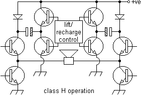
Class H designs switch in a higher voltage supply rail to cope with peaks. The basic arrangement for the Philips TDA1560Q IC, intended for automotive use, is shown below.
A novel approach, 'class S' (below), showed that if the load presented to the voltage amplifier by the power output stage appears very high, cross-over distortion can be reduced and the voltage amplifier is much easier to design.

Class T is a variation of Class D introduced by Tripath, where the pulses are modulated based on the individual characteristics of the output transistors.
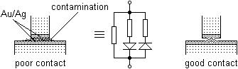
Connectors, switches and other mechanical contacts in controls can introduce anything from a faint crackling to an open circuit, a good contact only being possible when one contact breaks the surface of, and penetrates, the other, consequently causing problems when worn or dirty. At low signal levels, the consequences are obvious. Electronic switching, although sometimes complex, can overcome these difficulties.
It makes sense to position the stages where most amplification (and/or equalisation) takes place as near to the source as possible, eg; a record-deck fitted with a RIAA preamp. In an electrically noisy environment, a higher output will sustain a comparably lower noise floor than a much smaller signal. The number of switches and connectors that can degrade the signal is also reduced. The deck can, if desired, then (via a volume control) feed a power amp directly.
Some designs used PCBs with edge-connectors where the units were based on a set of PCB cards that could be slotted in and removed easily. This made the system quite flexible to manufacture and meant that any units sent for repair could often be ‘fixed’ quickly by relatively unqualified staff simply by swapping faulty boards which might then be repaired by a more experienced engineer using a dedicated rig. Examples include the Leak Delta and Armstrong 400/500 series. Unfortunately, these connectors could corrode or oxidise, themselves giving rise to failures. This corrosion could be caused by the fingerprints left by production and service staff. In this type of construction, attention given to these connectors in a non-functional unit will often restore it.
Destructive connector problems can arise when a power amp is split between PCBs like the 2 used in the Radford HD250, the 3 in the Powertran JLH 70W Deluxe and the 2 in the RSD 800b although the latter used a high-quality multi-pin connector whose pins were paralleled.
A DC presence can cause noise in controls, to avoid this AC couple any pots, particularly volume controls. In an older design this can be indicative of leaky coupling capacitors which should be replaced.
Magnetisation of tape heads could introduce hiss and crackling. Tape repeatedly passing magnetised metalwork can lose it's treble content. The Beocord 5000's bias oscillator would damp on shutdown, degaussing the record head automatically.
Electronic hiss is usually associated with Johnson noise, which is normally dependent on the temperature of an electronic device and it's associated impedance, or resistance, which can change with it. The more circuits in series (say a preamp, tone control and filter) the more hiss. On a mixing desk unused channel's noise can be used to cancel the noise in those used thus making the system quieter and increasing it's dynamic range.
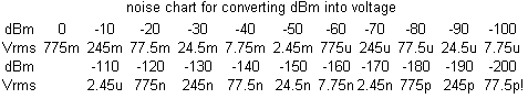
As with distortion, noise figures can confuse, unless one is an engineer, which most music listeners are not. Differing standards involving filtering can appear to offer lower quoted specs which can appeal to marketing, eg;
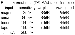
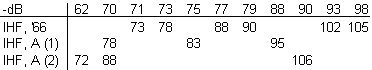
Low-noise amplifiers usually refer to an input load impedance to describe their noise output, whilst others give a measured mean voltage and bandwidth. Simply stating an A-weighted figure without a reference can be deliberately meaningless, as can measuring the output when the input is shorted. In the course of building preamps, a means of quantifying noise output was required and a relatively simple means of obtaining comparative measurements is described here.
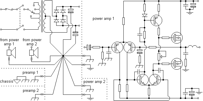
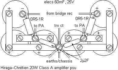
Power supplies can be considerable noise generators, the importance of mains filtering cannot be underestimated, many commercial designs suffering as a consequence of an almost mandatory and complete absence. 2nd and 3rd line harmonics can be very annoying as can by-products of rectification. 'Barrier' techniques, like those shown below, can be very effective, the first from a class A amplifier reducing noise by 20dB.
Pre-regulation, ie; running say 15V regulators from 24V regulators, in conjunction with plentiful smoothing is advisable for low-noise designs, although batteries are useful for critical low-level applications. Some 78x/79x series regulators can be very noisy compared to adjustable types like the LM317/37 types. A post filter of a 10R resistor and a 470µF-1mF electrolytic can help alleviate this, although discrete designs can arguably outperfom ICs in this context.
It is important to add supply by-passing to a stage's supply rails to reduce noise. Often, with opamps this is done with a 0.1µF ceramic cap and a 100µF electrolytic per supply rail. Some fast opamps, like the AD797, require the usual ceramic but also a tantalum of 4.7 to 22µF whose lead inductance is loaded with a carbon resistor of 1.1 to 4.7 ohms when driving heavy loads.
Hum can have a number of origins - inadequate screening, earthing or supply smoothing. All connecting media must be sound and clean. Steel is recommended for all cases and a maximum distance should be made between any transformers and low-level circuitry. For example, the integrating of an mains on-off switch and high impedance volume control may make ergonomic sense but may increase susceptibility to hum. Additional screening between these or around the low-level circuitry can help. Employ star or spider earthing (bringing all earths to a single point) throughout to prevent circulating currents.
Observing symmetry in supply arrangements will avoid audible ripple, earth connections to multiple smoothers often being made with a single plate.
If a connection causes an earth loop (disconcerting hum), disconnect one of the concerned grounds. A colossal hum, accompanied by a chorus of radio stations, usually indicates a disconnected signal earth. Some equipment is fitted with an earth-lift switch which isolates the signal ground from the (safety) chassis ground. Some 'separates' designs will have, say PCB selectable, ground options. If a ground is lifted, an HF path to chassis (capacitor) usually improves and is best made permanent.
Mains-borne noise, especially spikes, can cause annoying clicks, bangs and even destroy speakers and components. A solution is considered here. Care should be taken to ensure that prior to any switching, a resistor grounds decoupling capacitors so that no DC shift, due to leakage, produces transients.
Half of the 'fun' involved when building an electronic project for the first time is making it work when completed. Oscillators won't oscillate and amplifiers may do nothing but. Sometimes the cause of misbehaviour will be obvious, sometimes not. Reactive loads, for example, can cause all sorts of problems (see amplifier protection). Thermal drifts may be masked by hysteresis.
If embarking on a new build or repair, some useful advice is given in setting up an amplifier. If no 'scope or frequency meter is available, oscillation may be hard to spot. However, if a power amplifier (other than class A) runs hot, components start 'cooking', bias is excessive, next door appear to be using their electric drill a lot or radio breakthrough occurs and no obvious DC bias is present on the output, the chances are that there is a problem in this area. Check the RC network (Zobel, Boucherot) between the output and ground, if fitted, for open circuits (many manufacturers insist on a feeble resistor in this position). If this checks out, look at the small decoupling caps near the class A driver (if class A, AB) or the input devices (usually small ceramics) for open circuits. If no means is available to test these, simply replace them. Similar symptoms can arise from dry joints or cracked tracks, so check for these first. The class A driver, if replaced with a type with a higher than intended Cbc (say, 1-5pF), can give rise to oscillation. V-FETs can oscillate if their gates aren't loaded with resistance or if their supply runs are (relatively speaking) high impedance. Low value ceramic (low-inductance) supply decoupling caps (usually 0µ1F) should be mounted as close to the output devices as possible.
Consideration can be given to the drift of a capacitor's value with temperature (High K) and lifespan when mounted in close proximity to a heat source like a heat-sink. Choose a high voltage type, say 1kV for supply decoupling, and use more than one per PCB track.
Oscillation can occur when a test instrument's leads (DVM, 'scope) are applied to the unit under test. To prevent this, load the probe attached to the signal side with a resistor, say 680R. HF problems can cause equipment to radiate over a large area and must be avoided, often by law. Whilst steel is recommended for screening, care must be taken if equipment is dismantled and then unshielded.
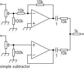
When dealing with PAs say it can be useful to subtract the input from the output. Artefacts, like cross-over distortion and oscillations, can then be easier to spot with a variety of frequencies and waveforms.
If a design, particularly one with a wide bandwidth, proves problematic consider whether capacitors intended to limit the bandwidth may be interacting, eg;
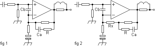
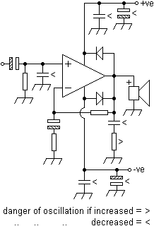
In fig 1, Ca may be included to counteract coupling between the input and output. Both Ca and Cb may not interact on one build but will in another. Reversing the RC network (R-Cb, fig 2) will place R between them reducing the interaction. Alternatively, Rx can be fitted. A small value, say 68R, should suffice.
With compact builds the PCB layout can be a cause of instabilities necessitating the use of extra compensation caps to damp oscillation which may only arise at high levels of volume. This can be caused by high magnetic fluxes inducing currents in high impedance low-level areas. As a consequence, keep a distance between the inputs and the output/supply rails. If this is not possible, put a screen between them. Some cases have been seen where an improvement in distortion has been made by running the supply wires (twisted together) perpendicular to the plane of the PCB over a few inches. Instabilities can arise when high current earth wiring follows the same path as that used for low currents.
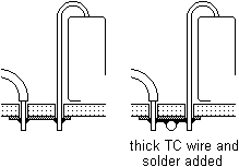
Sometimes the problem may only be apparent intermittently when high currents are passed through, say, a thin PCB track. A length of tinned copper wire soldered along the track's entire run can help prevent this, although all tracks on a new PCB should be tinned as a matter of course. Such steps are recommended for all high current runs in new builds before populating the rest of the PCB. Older, especially commercial, designs can benefit from this modification also.
Small value capacitors should be mounted close to their associated components keeping track lengths as short as possible. Self-inductance will increase if leads are bent. If a long track length is unavoidable (>20mm), this should be at a low operating impedance, or have a multiple path. The inductance of long tracks in conjunction with a capacitor can form a very high Q LC tuned circuit, and the oscillations produced will have a worse effect than not having any decoupling at all. This is particularly true of supply and ground connections - a simple jumper wire connection, rather than a copper track, to a single logic IC ground caused enormous difficulties for one constructor.
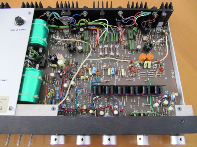
Similarly, mount transistors close to the PCB. Long lead lengths can induce a variety of HF/VHF problems, especially if associated with high impedances, gains and currents adding to colourations. The view below shows how not to layout an output stage, although such occurences may be more down to the manufacturer's production team, rather than the original designer. Output devices with a low fT can probably cope with long runs like this but if the author was presented with an unstable new build of this format a reduction in wiring length would be on the cards.
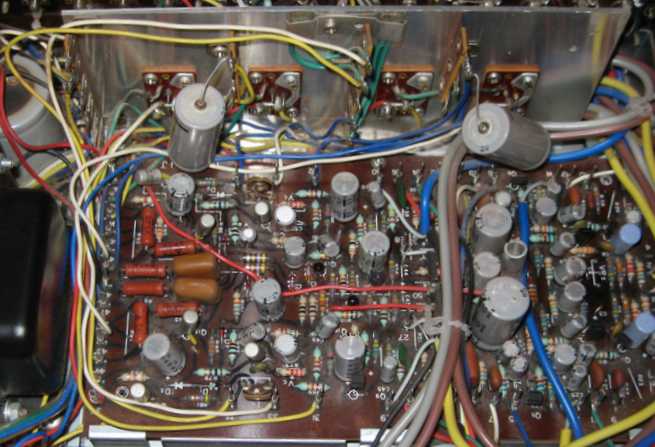
Another design whose PA PCB tracks could have been rotated 90°. Note also how the PA input leads (white) snake around the board and are then held in place by unrelated components. The signal path should flow topographically from input to output.
Some ICs, whether opamps or regulators, can become more prone to instability at higher operating temperatures, particularly if of commercial grade. Loading the inductance of the leads of a tantalum capacitor with a low-value carbon resistor might be required in bypassing some high frequency opamp's supplies. The voltage dependence of a ceramic type's value can give rise to unwanted changes in frequency response, especially if used in feedback paths. For this reason, polystyrene types maybe preferable.
If mounting axial-leaded resistors in an upright position to reduce PCB area, the longest lead should be connected to the least impedance 'seen', thus reducing the area of a 'sensitive' high impedance side. The same can be said of polystyrene caps which if marked at one end indicates that wire is connected to the outermost foil and is then ideally connected to the least impedance.
Components exhibiting intermittent faults (which can have the highest annoyance level), say on warm up, can sometimes be identified by tapping with an insulated object, cooling with freezer spray or gentle heating with a small soldering iron brought into close proximity to them.
Sometimes the source of fault may be in an ancillary circuit, like a protection circuit, and not the amplifier - "There was no DC triggering the circuit from the emitter resistor. It was cross talk and leakage – and only happened in musical transients as you can get a net DC level – high impedance trigger input and boom – false trigger. Turned out the (DC) V Sense transistor was floating – some track break that could not be seen – and I obviously failed to measure. I double tracked the PCB around the area and it works fine. If I had listened first, I would have realised that there were no cracks or pops in the music as the triggered fired – hence no odd DC sifts etc. Relied too heavily on a scope!".
Full bridge amplifier designs increase the chances of HF instabilities. Ensure that a very low impedance ground exists between both amplifiers and that the DC offset of each is as close to zero as possible. Although useful for say doubling the slew rate and increasing output power, experiments with these are best left to experienced constructors since double the damage can occur.
As noted above, destructive connector problems can arise when a power amp is split between PCBs or if long wiring runs are involved in the power stages. For this reason, it is recommended that new designs be built on a single PCB or substrate. If a multi-way connector is unavoidable choose a multi-, say 3-row, type with as many pins that will fit the PCB and parallel the pins in adjacent rows - the more the merrier. Select a hard gold-plate with high current rating (2A+) with as low a contact resistance as possible, say 15 milliohm.
Much of the travel on an average volume control is redundant, most domestic amplifiers giving a sufficient volume at about '2', with objectionable distortion, either of amplifiers or speakers, occuring long before the end stop. If the gain of the power amplifier is reduced to suit and set below clipping at all normal preamp settings of the programme material at the maximum volume setting, bandwidth will be increased. The amplifier will then be better able to tackle nonlinearities. At the same time the input referred noise floor will be reduced and the signal to noise ratio will improve.
Many preamps will supply signals far in excess of line levels, some at 10 or even 20V. Accommodating and even using this will further reduce contributory noise levels from power amps. To this end, some users have impedance converting amplifiers, in some cases having no voltage gain or feedback.
Contact me at paulkemble@hotmail.com
especially if you want additional content to this page
or if you find
any links that don't work. Don't forget
to add the page title or URL. Take care!