Offsetting an audio amplifier
Differences between the two halves of a differential, or long-tailed, pair can be amplified resulting in a strong DC bias appearing on a directly-coupled output. These are not only wasteful but can result in non-linearities contributing to distortion and even the destruction of speakers. Common-mode rejection (in this case of the ripple on the supply lines) is similarly affected. A (below) shows a typical arrangement where the input offset voltage is related to the base-emitter voltages of the input transistors.
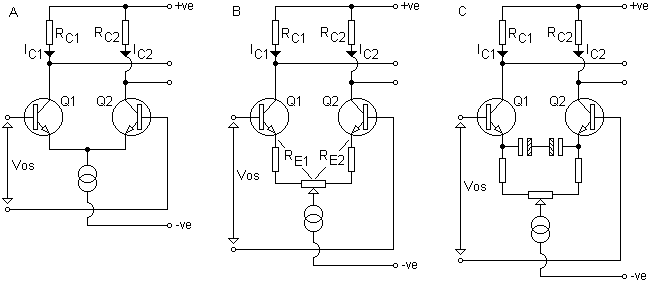
The differences between additional emitter resistances (B) can be balanced by a potentiometer, however, gain can be reduced although this may not be important. Lost gain may be recovered by the use of bypass capacitors (C) across the emitter resistances.
Ideally, both transistors and resistors should be matched and in thermal equilibrium. For example, TO92 style cases can be bound together with a copper band (offering some thermal regulation), or alternatively, dual differential pairs can be fixed to a copper plate, or block, which can be earthed, a smear of conductive paste being placed between the mating surfaces, an approach very rarely seen even in 'high-quality' commercial designs.
A similar arrangement was used in the Practical Electronics Gemini to bind the bias and driver transistors together.

Differences can be made almost insignificant with the use of dual transistors or a monolithic IC differential stage. A close match between discrete transistors is, however, unlikely. Thus, a DC amplifier's offset's tendency to increase over time.
In symmetrical amplifiers, associated transistor pairs should ideally be matched, complementary pairs (NPN/PNP) may then be required, matched both in Vbe and hFE. A relatively simple transistor matcher is described by Giesberts (elektor, 7-8/'97, p98-9).
Resistors can be matched by using high tolerance types or measuring them. However, it is often sufficient to take, say, four successive resistors from the 'belt' in which they are packaged.
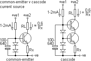
The performance of a constant current source, which importantly helps to isolate supply noise from the 'tail' or say a class A driver, can be improved by adding an extra transistor, the output characteristics of the cascode circuit approach those of an ideal current source much more closely than those of the single transistor circuit.
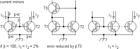
Similarly, in a current mirror, a third transistor can be added to reduce the error by a factor equivalent to that transistor's current gain. Ideally, as with a differential pair, these should be identical, ie; on the same chip (CA3046/86, etc).
Many approaches, for simplicity's sake in a real world, dispense with offset adjustment altogether and use a capacitor to decouple the DC feedback path to ground, thus reducing the amplifier's gain as it nears DC. Residual voltages on the output would then typically be below ±50mV.

The time it takes this capacitor (usually a single electrolytic) to charge and discharge can result in large near-DC swings appearing on the output. Particularly noticeable at high outputs, bass notes tend to lose definition. The quality of the capacitor chosen can also affect performance at high frequencies. To overcome this, some designs will use, say, a 10µF polypropylene type. Feedback impedances can then increase, but this may not be significant in subjective terms.
Alternatively, if single op-amps are used then conventional off-setting can be applied. This has been used in designs where fuses have been placed in the supply rails, rather than the output (non-linear resistive effects at low frequencies).

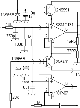
An approach that one could find in a lab is shown below.
This demonstrates a distinct reduction in the number of capacitors in the signal and feedback paths.
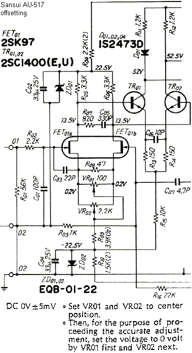
One manufacturer took pains to match their input transistors (below) and enclose them, thus isolated from their surroundings but coupled thermally.