Hitachi FET amplifiers.
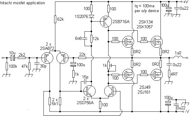
This design ranks as one of the simplest mosfet designs seen and given it's performance versus it's simplicity, has spawned a fair number of copies and derivatives (application kindly sourced by Alister Sibbald).
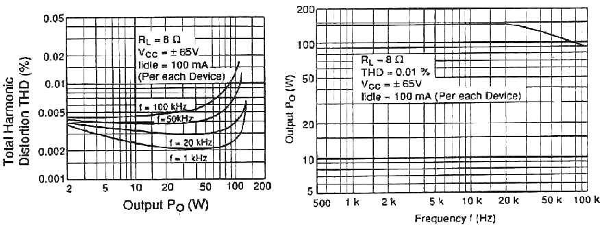
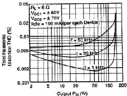
Performance graphs are shown below.
Output devices were easily paralleled (with their attendant gate resistors) for higher power handling, 100W output devices being specified for both designs; either the (140V, 7A) TO3 2SK134/2SJ49 or the TO3P 2SK1057/2SJ161 which are more expensive but are arguably easier to mount. These had an Rds of 1R7 each. Other devices like the TO3P (140V, 8A) 2SK413/2SJ118 or the 2SK414/2SJ119 (160V,8A) had an Rds of 0R5 (Rds = Vds(sat) / Id, eg; 2SK134/2SJ49 = 12/7 = 1R71). Employing a lower Rds can give rise to lower dissipation in the output devices and allow the use of a lower voltage supply and/or a smaller heat-sink, eg; ±57V6 instead of ±65V for 100W/8R.
The drive power requirements for a FET are smaller than that needed for a bipolar device the only energy required, which increases with frequency, to charge/discharge the gate-to-source-capacitance. At 100W and 100kHz this would be

so the components for a class B driver stage are not required, the drive being taken directly from a class A predriver, normally found in a bipolar amplifier.
Ideally then, a low Qg (total gate charge) and low Rds(on) are desired for the best amplifier performance. Unfortunately, these are conflicting requirements since Rds(on) is inversely proportional to Qg for a typical MOSFET. The design trade-off is one of cost versus performance. A lower Rds(on) means lower I^2Rds(on) losses but the associated higher Qg translates into higher switching losses (losses = Qg x 10 x 1.2MHz). A lower Rds(on) also means a larger silicon die and higher cost. A higher Rds(on) means lower cost and lower switching losses but higher I^2Rds(on) losses.
Other advantages accrue from using FETs. Bipolar transistors have a negative temperature coefficient, which means that as they heat up they pass more current, thus getting hotter, FETS have a positive temperature coefficient which means that the current they pass reduces as they heat up and, because of their architecture the heat will be spread over the entire chip instead of confined to hot-spots as in a bipolar type. These devices then have an inherent safety feature built in as far as internal dissipation is concerned. As a consequence the bias thermal stability or 'variable zener' circuits normally found in bipolar output stages, that themselves give rise to distortion or even stage failure, can be omitted also. The simplified layout precludes the use of a bootstrap capacitor as well.
Any reduction in the component count, especially in the output stages, will not only reduce cost, and any attendant distortion, but can also increase reliability and improve sonic performance since there is less to 'get in the way'. This has probably been the reason why this design has been favoured and adapted by many, including the author. In keeping with the rest of the approach, the bias pot should be a high-quality type.
The transconductance |yfs| of power FETs (1-2.5S) are a fraction of those for a given bipolar type with an Ic of, say, 1A.
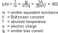
In an emitter/source follower the relationship between input and output is expressed as Rl / (Rl + 1/|yfs|), the non-linear part, |yfs|, causing distortion. Thus a FET can distort at levels 20dB higher than a bipolar type. To overcome this, a larger than usual open loop gain and more negative feedback are required, compared to a bipolar circuit.
Due to the high frequencies of which these devices are capable ('almost embarrasingly so compared to bipolar type's according to one designer), advice to avoid parasitic oscillations was provided; mounting the output devices directly to a PCB, single-point earthing, substantial supply and output wiring, the use of a output inductor to be determined experimentally and that the PCB should 'flow topographically from input to output'.
A second more complex version using FETs throughout was also described. This was a DC design with low-impedance offsetting applied to the input pair, with stabilisation of their feeds and a separate supply for the input and driver stages.
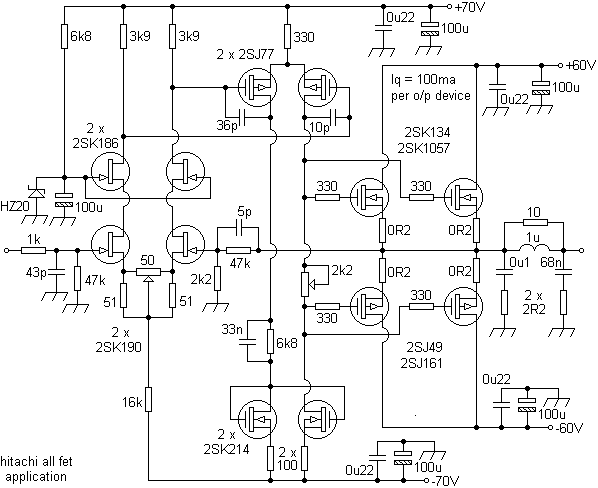
This gave a slight increase of THD at high frequencies.
Alister notes that
"For whatever reason, the thing worked very well. I was doing an MSc in the Audio engineering lab under Malcolm Hawksford at Essex University at the time. We knocked some up and were quite taken aback by how good they were - especially as we were in a 'mode' with our designs to see just how complex we could make them. The Hitachi Mosfet datasheet (and thinking back, it must have been early '80s) generated a host of copies. The Maplin Mosfet amp kit was well known. The current BK Electronics modules look as though they're based on it and there were innumerable commercial clones. It's one of those very simple circuits (like JLH's 10W class A) that somehow just seem to get it right. Particularly, as we found in Hawksford's lab, if you use two of them as a "Balanced" amp - a finding which set some of us off on a search for the "Earth effect" on the assumption that the improvement was largely down to balanced connection keeping high currents out of the earth connections. Malcolm actually published a number of AES papers (the "Pontoon" amplifiers) triggered by our investigations of these Balanced Mosfet amps."Compare to another Hitachi design which uses a 'different' layout and the earlier Yamaha B-1.
especially if you want additional content to this page
or if you find any links that don't work. Don't forget
to add the page title or URL. Take care!