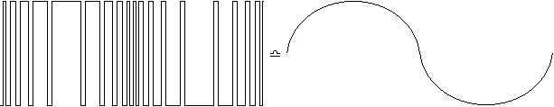
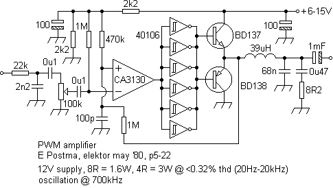
"The entire amplifier oscillates and produces a square wave. This is because one of the inputs of the opamp comparator is connected to the output by means of a RC network. Both inputs are biased to one half of the power supply. Whenever the opamp output is low and the transistor emitters are high, C is charged and the + input rises. If this rises above the level of the - input, the output swings low to high and the transistor emitters swing high to low. C discharges to the output, the voltage at + drops below the - and the output of the opamp switches back to a low state. The level at -, used as a reference, is determined by the input. The point at which the comparator changes, is also determined by the amplitude. As a result the width of the square waves is constantly changed (modulated) by the audio signal." - elektor (condensed)
A stereo pair of these were built (PCB 80085), the output devices requiring no heat-sinks. Listeners did not recognise or identify anything untoward in the output produced, though limitations were obvious at high levels. Indications were that good quality hi-fi could be achieved with switching frequencies ten times, or more, higher than that required by the system's frequency response. These could be as low as 250kHz (adequate telecom quality with 125kHz) with an upper limit of 1MHz or less (governed by practical output stage topology).
It was clear that a smaller power supply than normal would be required, although regulation (series pass) was provided for each amplifier to overcome the on-offload regulation of the smaller mains transformer and any attendant noise (eg; beat frequencies from other channel) carried by the supply. A comparison of conventional supply arrangements for a class AB and a class D design of similar output is given below.

A solar-charged lead-acid system showed less strain compared to another class AB system, demonstrating usefulness for critical situations. Power supply noise was not obvious with either supply, presumably because of the low impedance and the amount of smoothing and decoupling employed (10mF + 4.7mF & 1µF per PCB).
Increased output power was an obvious 'next step' and a Bridge Tied Load or BTL configuration, using both PCBs and meatier output devices (possibly driven by the existing ones), was considered (below) but not pursued. This was expected to yield >30Wpk into a 4 ohm load with the same 12V supply.


Possibilities suggested included light, but powerful, mobile designs utilising MOSFETs or low current designs (head/earphones) using logic ICs. Domestic and professional amplifiers are dramatically reduced in size and active speaker designs are now easier to implement, the amplifiers housed internally, there being no heat-sinks to ventilate, thermal losses from the speaker being greater.

For large speaker loads a heavy-duty, fast charge pump could be employed. A combined mains power and output stage was envisaged. Output and supply stages then become easier to implement, using fewer and smaller components, even conventional mains transformers becoming redundant. Although no protocols were then readily available, such a system could be driven by infra-red, the drivers being coupled even remotely.

A compact integrated switched mains power supply and amplifier module was considered, commonality of components aiding, for example, active speaker system assembly and servicing. A design employing components rated for a (former) UK 3 phase voltage of 415V will function world-wide. With no height of conventional mains transformer or length of heat-sink to consider, very appealingly slim designs were possible.
It is feasible to make judicious use of industrial PWM motor control (50kHz) to drive large bass loads. For those interested in this approach, experience suggests that 'leakage' to ground (via a 1M resistor) between combined but isolated control/drive/output stage's grounds, can prevent build-up of catastrophic static when PCBs are mounted 'back-to-back' (presumed back-EMF from motor being stored between the copper planes). Failure of under-rated snubber circuits across main switching devices can precede this.
At about the same time, a welding set whose spark was modulated by an audio signal suggested a new approach to spherical acoustic radiation patterns, although definition, especially that of bass, was severely limited. A melding seemed possible. A similar principle was demonstrated by Magnat's [Wagner & Wagner 1980] Corona Plasma loudspeaker - a 27MHz oscillator of 20W was amplitude modulated by an input which then was used to generate a high voltage developing 15,000°C at a needle point giving an output of 3kHz to 200kHz at 114dB in all directions. Time and resource, however, could not support implementation of such designs, so a decision to await developments in hardware was taken.
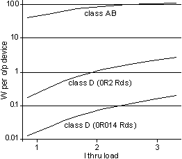
Output stage losses appeared to be due to resistive and switching (dynamic dissipation) phenomena, this last restricting the upper limit frequency of self-oscillation. Resistive losses can be approximated by (P out / R load) x 2 x output device Rds x temp coefficient factor (eg; 1.3 for FETs). For example, if a 6R speaker is expected to carry 50W and the output device Rds is 0.18R, then the amplifier power loss can be (50/6) x 2 x 0.18 x 1.3 = 3.9W. Compare this to a class AB or a thermionic design. Obviously, if output FETs with a lower Rds are used, losses will fall even further, eg; if Rds = 0.014R, loss = 0.3W.
Ideally then, a low Qg (total gate charge) and low Rds(on) are desired for the best amplifier performance. Unfortunately, these are conflicting requirements since Rds(on) is inversely proportional to Qg for a typical MOSFET. The design trade-off is one of cost versus performance. A lower Rds(on) means lower I^2Rds(on) losses but the associated higher Qg translates into higher switching losses (losses = Qg x 10 x 1.2MHz). A lower Rds(on) also means a larger silicon die and higher cost. A higher Rds(on) means lower cost and lower switching losses but higher I^2Rds(on) losses.
Switching losses (both output devices conducting simultaneously during transition) can be reduced on some new designs by programmable timings. Simply monitor the output stage supply for a minimum quiescent current, about 6mA or less, with no input signal if adjusting these. As with the self-oscillation frequency, an over-lapping of turn-on times may drift with temperature and supply voltages, though not necessarily to a critical extent.
Sometimes a compromise is required between the sonic performance of a design and it's efficiency. The dead-time that is allowed between the output device's conduction can determine the efficiency of a design to a great extent; a long dead-time leads to higher efficiency. On the other hand, long dead-times can worsen sonic performance and have important adverse consequences, for example, for the THD. A short dead-time causes the quiescent current to rise, thus reducing efficiency but improving the sonic performance. The higher quiescent current is the result of more cross-conduction of the output devices. Most of the power that is lost in this way is then
dissipated in these, which may heat-up excessively, then causing undesirable thermal instability. For this reason, during an initial evaluation say, the risk of damaging the output devices through thermal runaway will be reduced by using a low quiescent current. In some designs, notably discrete ones, the dead-time can be shortened by modifying one resistor value. Changing this, for example, to a lower value may decrease the dead-time. To reduce the risk of thermal runaway in an enhanced sonic performance mode, a thermal feedback loop can be used. The operating temperature of the output devices can be fed-back to the dead-time control by changing the resistor's fixed value. This can be done by mounting a PTC resistor on the heatsink and connecting this in parallel with the resistor.
For all practical purposes, input and driver circuitry supply losses can be ignored, this being governed by it's complexity. Altogether switching and control losses can amount to ¼W per output stage, or even less.
Transients arising from the output inductor when both transistors are off can be dealt with by Schottky diodes clamped across them.
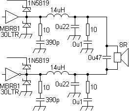
The inclusion of an output LC filter to block the square wave simplifies construction and dramatically reduces distortion, presumably arising from the overshoot of the square wave caused by the inductance of the speaker. The use of an output filter means also that the speaker is then not required to dissipate an inaudible square wave. A reduction of radiated RF harmonics will also result. The Q of this filter (0.7-2 recommended) can affect sound output quality; too low and output noise will increase, too high and peaking may occur at high frequencies. To accommodate 4-8 ohm loads, engineer for 6, eg:
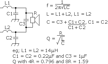
AB output stages usually include an inductor of 3-5µH, class D stages need coils with a value maybe five times or more higher. These can be cored to reduce bulk, but those that exhibit hard saturation should be driven well below their saturation current, eg; the Toko 16RHBP-140M (14µH, 4.9A) has been specified for a PWM design intended to drive 8R at 40W (<2.3A). Screening of such coils is recommended since these can radiate at RF. A 'Loudspeaker Passive Crossover Choke Coil Calculator' can be found here.
Today, with the advent of Surface Mount or Small Outline devices, the technology has certainly come of age and complete amplifiers of some sophistication are offered in packages that compare favourably with that of a single medium-power transistor (chip even), heat-sinks required only if continuous high outputs are run. At the same time, many useful features such as current and thermal cut-outs, mute, standby, etc, are included rendering remote control and monitoring possible. For miniature applications, the TI TPA2028D1 offers a 3W mono, filter-free Class-D audio power amplifier with volume and optional I2C control, dynamic range compression (DRC), automatic gain control
(AGC) and is available in a 1.63mm x 1.63mm wafer.
'Over modulation' protection is given in some designs by a minimum pulse time providing a 'soft-clip' to the top of a sine wave. This can mean that, albeit over a narrow region, a class D amplifier can sound cleaner than a class AB design when driven into clipping. Some allow for easy synchronisation to prevent beat frequency interference when using several amplifiers on the same supply.
A preamp might be required to drive some ICs. This can consist of a filter (to determine the power amplifier's frequency response) followed by a gain stage (say x10).
As of 2005, an excellent introduction is Maxim's app note 1760. As other companies do, they also offer an assembled surface-mount evaluation kit for their low-voltage MAX4297 IC (250kHz, thd + n = 0.4%, 2W @ +5V, >83% efficient).
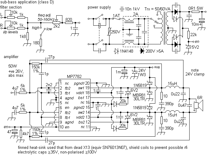
Performance comparable to a class AB of about 50W is offered by the MPS MP7782 (400-600kHz, thd + n = 0.06%, >90% eff) and the Analog AD1994 (thd + n = 0.005%, >80% eff). A meatier solution is National's LM4651 & LM4652, offering 170W (@10% thd, ±22V @ 10A) in two packages, the output pairs (LM4652) being packaged separately from the control circuitry. A filterless solution is offered by the Microsemi LX1725 (15+15W, or 30W mono). These invariably operate in BTL, or 'H', configuration ie, the speaker is fed by two output stages each being antiphase to the other (see above).
Since it is easier to make N-channel FETs with a low Rds, compared to P-channel devices (in the same way it is easier, in silicon, to manufacture NPN transistors as opposed to PNP), there is no reason why outputs cannot be of a 'quasi-complementary' design. For discrete output stage designs, the IRF6665 has been suggested as an ideal MOSFET for a medium power class D amplifier, although the HUF75337P3 'Ultrafet' (62A, 55V, 0.014R, -55 to 175°C, 115W, TO220) is worth a look for designs intended to sink in excess of 20A. A possible partner for these might be the LM4651 (driver stage). The IR TO-220 Hexsense FETs, like the IRC540/640/840, provided a current sense output for monitoring/protection.
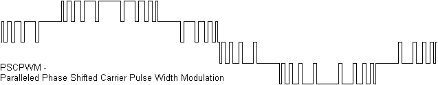
Complete modules, with on-board mains supplies that can supply other modules, can be found at ICEpower. The same company also offers implementations involving paralleled output pairs utilising Paralleled Phase Shifted Carrier Pulse Width Modulation, or PSCPWM, which can potentially offer higher output handling using smaller output devices, reminiscent of analogue class G. With two pairs a resultant waveform would be that shown below. With more, the waveform can be broken into finer steps.
Some evaluation kits seen can appear to underate components, for example, one device whose absolute maximum supply voltage is given as 26V has 25V caps specified for a 24V supply. In this case, specify 35V minimum for the electrolytics and 100V for the other caps, especially those on the power supply and output. This may seem high, but given the dV/dt involved some headroom is advised. Clamp the supply at 24V and run at about 20V, even 12V supplies being capable of giving a satisfactory performance (paralleled speakers).
Manufacturer's power ratings can sometimes appear oddly optimistic. For example, a 250W design will in reality have a continuous rating of 25Wrms and an amplifier offering 1kW (for 15 seconds, no preheat) will have a continuous rating of only 85Wrms. High power levels at high frequencies may then be limited by the output filter's and other safety circuits ratings, eg; 4% @ 20kHz compared to 100% @ 4kHz. Instantaneous power outputs can have relevance to a 'music' output, but can confuse when comparing component ratings. For example, a Zobel / Boucherot network across the speaker will be driven harder as a speaker's impedance rises. Caution should also be given to capacitive loads, given the extreme sensitivity that some designs have towards them. Exceeding some 0.47µF can cause oscillation (and shutdown).
Even though thermal management problems are reduced on a factorial basis with PWM, it should be remembered that even a small amount of heat-sinking (via the PCB) can dramatically reduce chip operating temperatures. A 20W load will, assuming 85% efficiency, dissipate 3.5W in a chip. This might well then run at 16°C above ambient with a thermal pad, but at 103°C above without (thermally isolated). Even though sensors may not come into play until 125°C is reached (with shutdown at 150°C), any component can be expected to last longer the less stressed it is, whether this be by temperature or voltage. Use has been made of finned heat-sinks from dead or redundant power amp chips, like the SN76003/13, etc. DIL heat-sinks being felt to be limited, PC CPU radiators have been sawn into shorter lengths and fitted.
Although complexity of design can become an issue and 100% efficiency is not possible, for compact or power starved situations, very acceptable performance can be achieved with the vast majority of listeners being unaware of any difference, class D designs appearing in 'audiophile' amplifiers. Very critical listeners have been unable to differentiate between class A and D designs and have been surprised to see a ratio of some 100:1 in terms of size, weight and cost. Personal preference considers PWM ideal for innovative active speaker designs, particularly as bass drivers. Self-diagnostics can utilise an output device's 'flags'.